Y. Palti, “
Complex Optical (Amplitude and Phase) Device Characterization Tool,” 2009.
Publisher's VersionAbstractOptical communications has experienced a rapid development during the last decade. More bandwidth can be acquired by decreasing the spacing of the optical channels or by increasing the data rate. Characterization of the optical components and active monitoring of the network calls for accurate measurement methods. The transfer function of optical components impacts
the performance of communication systems. Analysis and accurate measurement of the transfer function is therefore essential in optimization of the performance of such systems.
Chromatic dispersion of optical bers and frequency chirp of the laser transmitters set limits for the data rate and transmission distance. Measurements of dispersion have traditionally been performed using a Modulation Phase-Shift (MPS) method. When high RF modulation frequencies are applied to achieve high resolution an alias error could be introduced. In this thesis we introduce an apparatus for full complex-amplitude spectral characterization of optical
components and bers. Based on a modication of the MPS method, we introduce a frequency dither to the RF modulation drive, allowing us to detect small phase changes thus overcoming the limitations imposed by the conventional MPS method. Its salient feature is high sensitivity phase detection enabling the use of a low RF driving frequency as necessary for precise measurement of components exhibiting fine spectral features such as microresonators and slow light devices.
We analyze the modied MPS technique using the traditional small signal approximation and compare the results to a full analytic response of the MPS technique. The full analytic response is useful for optimization of the proposed technique. The characterization apparatus has been realized in our lab using commercially available optical and electrical components. We have characterized experimentally the signals passing in the apparatus. Care was taken to prevent higher RF tones (i.e. above 1st order) in the Mach-Zehnder Modulator (MZM) output field, which could interfere with the desired measurement. Moreover, care was taken to prevent RF leakages in the electronic circuitry, which could interfere with the measurement of weak signals. We demonstrate the operation of the modified MPS at two operating points, demodulating with either the same RF carrier or with a doubled one. We measured several component categories and fibers to demonstrate the measurement technique. Finally, we conclude with the advantages and disadvantages of the modified technique.
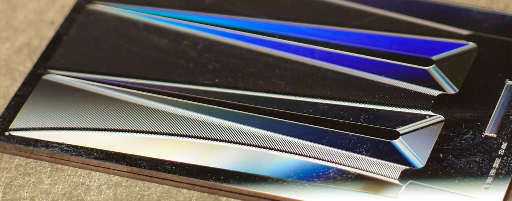
 Complex Optical Device Characterization Tool
 Y. Glazer, “
Novel Polymeric Waveguides Optimized for Nanocrystal Hosting,” 2009.
Publisher's VersionAbstractAt the last decade, the wide growth in data transfer realized the requirement of optical communications for its high capacity capabilities. The revolution of optical communications has been enabled by the availability of ultra-low-loss silica fiber, which has also been the basis for a wide variety of optical building blocks.
Fabricating passive optical devices from high purity silica and glass, or fabricating active devices that utilize the direct band gap of semiconductors (SC) are relatively costly; therefore alternative solutions are being studied widely.
Our research is aiming to realize a platform based on passive polymer materials as the wave-guiding material, and in the future to dope it with SC nanocrystals (NC). Plastic (polymers) optical fiber has already found significant application in the Datacom market.
In this work we present the design of optical devices and their fabrication. Polymer selection is critical, as most polymers have CO and CH absorption bands which reside near 1.55m wavelength. A PFCB core and a Cytop as cladding were chosen and combined together for the first time. This two polymers combination offers a very small attenuation at the optical communication wavelength of 1.55m, high Δn and solubility with NC.
At the design process, we focused on realizing devices that will help us extract the basic characteristic of our polymer platform, such as propagation losses, bend losses and reflective index changes that will occur after NC doping.
Realizing polymeric waveguides with a micron-scale cross section of and length of a few centimeters has low defect tolerance which requires careful treatment. Fabrication was done with standard semiconductor process, such as lithography, reactive ion etching etc. Furthermore, a low preparation temperature is critical when heat-sensitive elements, such as semiconductors nanocrystals, are to be embedded in the waveguide. Finally, after the process development, we have the desired polymeric waveguide structure. This waveguide platform is now ready for future study of NC dopants.
