Citation:
Abstract:
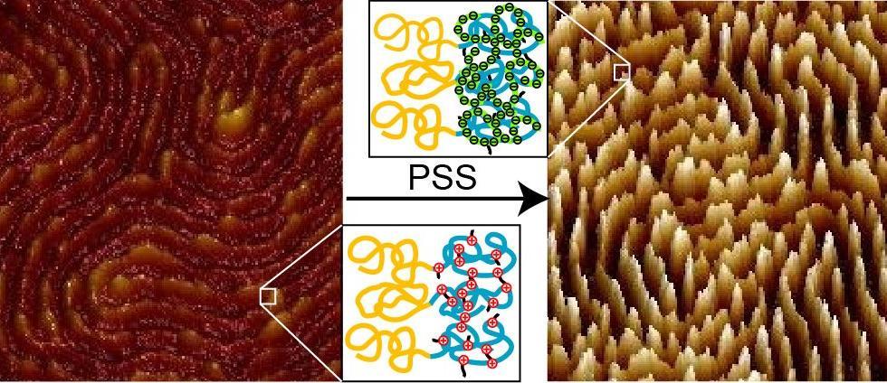
Nano-patterned materials are beneficial for applications such as solar cells, opto- electronics, and sensing owing to their periodic structure and high interfacial area. Here, we present a non-lithographic approach for assembling polyelectrolytes into periodic nanoscale patterns over cm(2)-scale areas. Chemically modified block copolymer thin films featuring alternating charged and neutral domains are used as patterned substrates for electrostatic self-assembly. In-depth characterization of the deposition process using spectroscopy and microscopy techniques, including the state-of-the-art scanning transmission X-ray microscopy (STXM), reveals both the selective deposition of the polyelectrolyte on the charged copolymer domains as well as gradual changes in the film topography that arise from further penetration of the solvent molecules and possibly also the polyelectrolyte into these domains. Our results demonstrate the feasibility of creating nano-patterned polyelectrolyte layers, which opens up new opportunities for structured functional coating fabrication.


